Keycard Shell is designed so you can check its hardware yourself. You don't have to take our word that your device is unmodified. You can open it, look inside, and compare what you see with the public design files.
Supply chain attacks and evil maid attacks exist. Someone can add a spying component to a device between the factory and your hands, or while it is out of your sight. This is true for hardware wallets, and also for your keyboard, your home camera, and any other device. No vendor can rule it out.
A common answer is to make devices hard to open: epoxy, sealed cases, or a wipe when the case is opened. We think this moves the trust to the vendor instead of removing it. You can't check a device you can't open, and you can't repair it either. A seal is a claim from the vendor, not evidence. Seals can be cloned or bypassed, and an attacker can get through most protections if the target is worth the cost.
So we designed Shell to be opened easily, repaired easily, and checked easily. Inspection is evidence.
Shell hardware is open source, and we publish it to manufacturing depth:
- Schematics and bill of materials, like most open hardware projects.
- PCB Gerber files: the actual routing of every board layer. This is what a factory needs to make the boards.
- Pick-and-place files: the exact position of every component on each board.
- Assembly drawings and 3D files of the boards and the case.
The hardware license lets anyone study, manufacture, modify, and share the design, as long as modified designs stay open. The files for production units are in the serial_run folder on GitHub ↗, and the main board of the first production is in the pilot_run folder (see Step 2).
Opening your Shell is easy and doesn't damage it. Watch the video for each step.
serial_run folder also contains V3.8, a later revision that only lengthens the USB-C connector pads. Both versions have the same components in the same positions. More about board versions ↗Take clear, well-lit photos of both sides of each board. Then choose one of these two options.
Give your photos to your AI agent, with a link to the Shell hardware folder ↗. You can use this prompt:
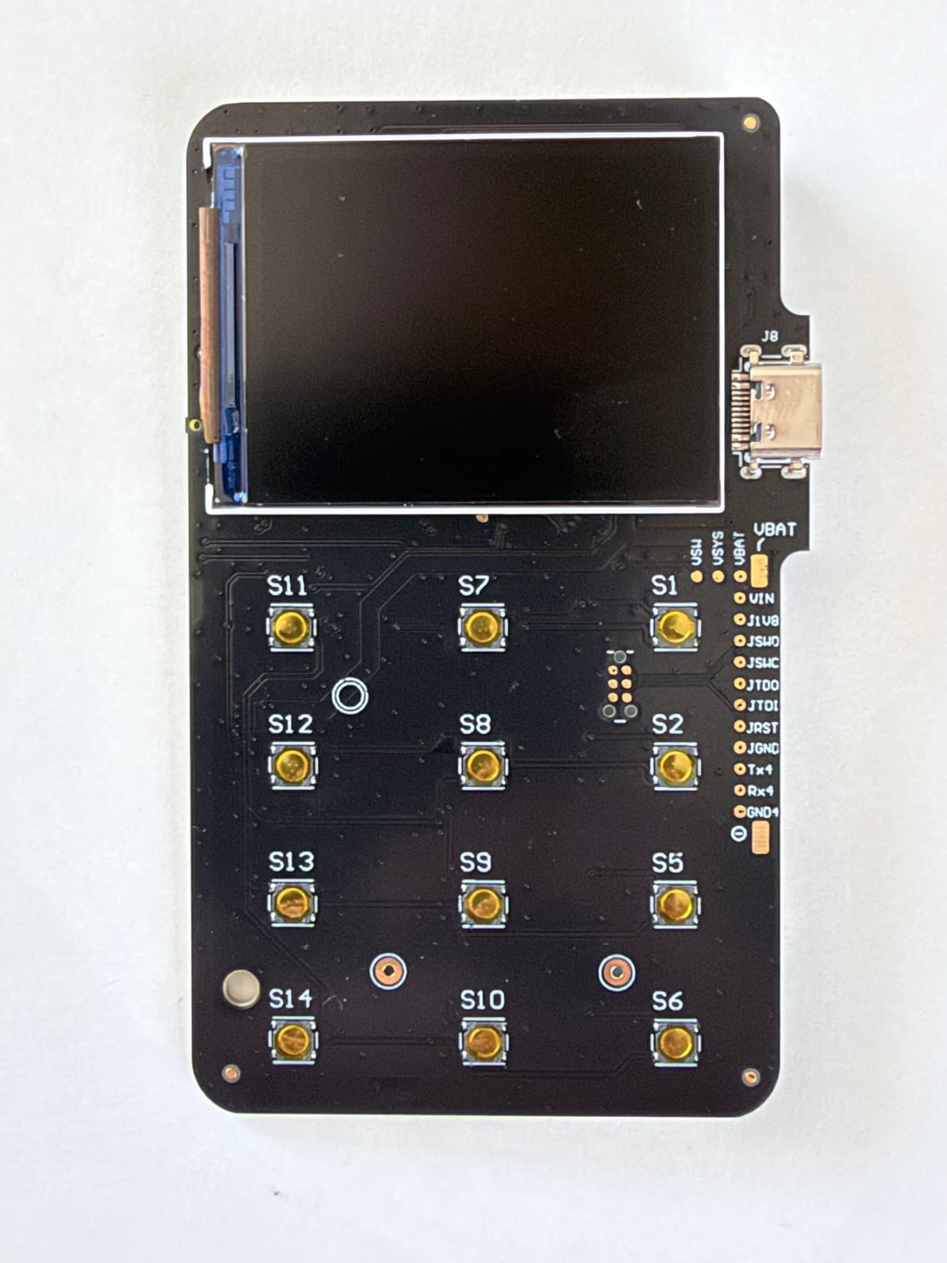
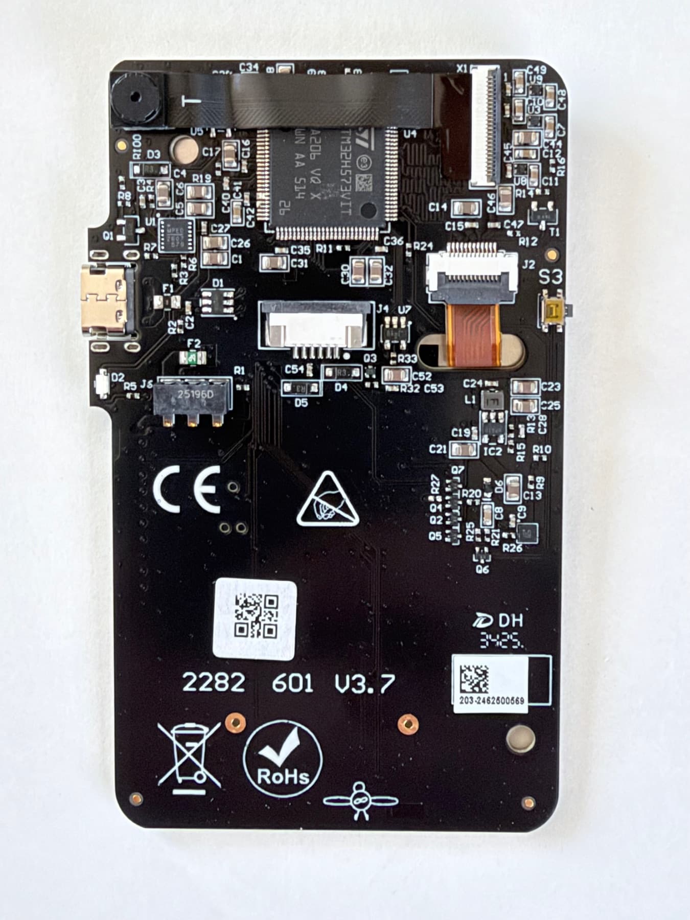
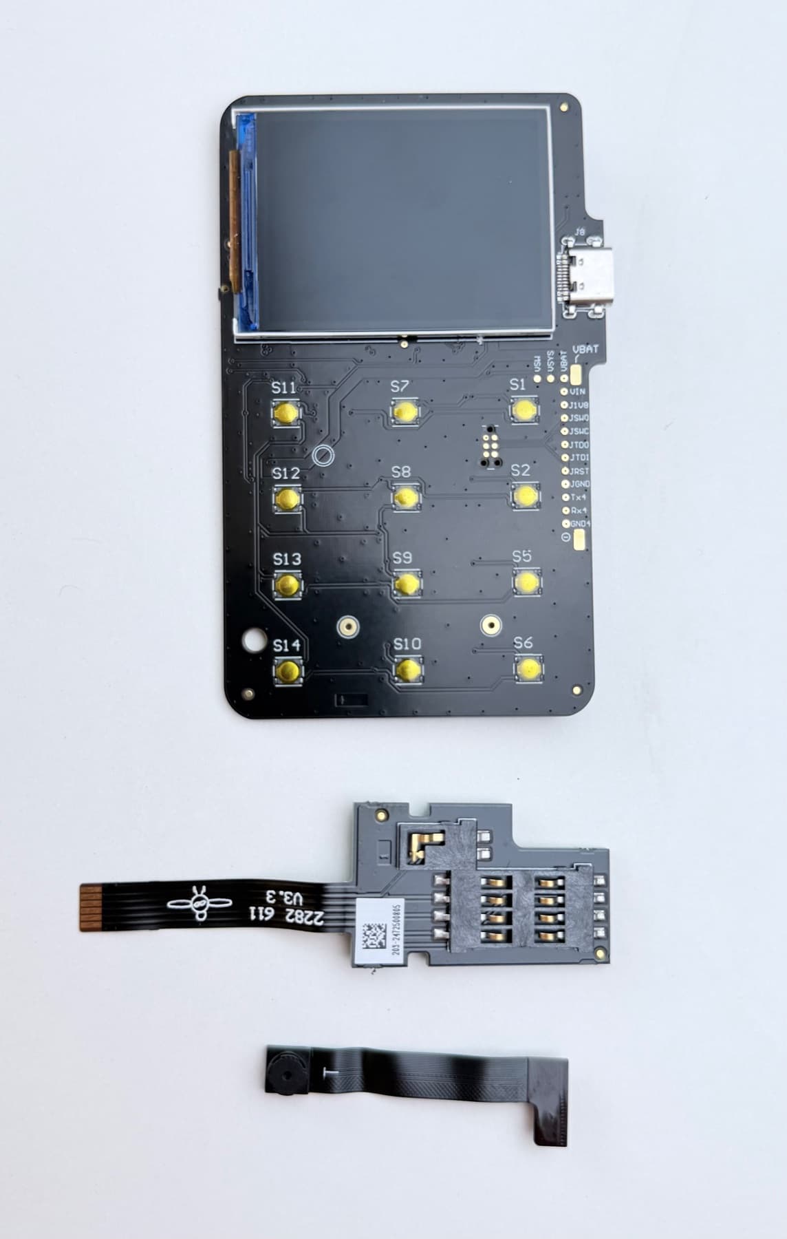
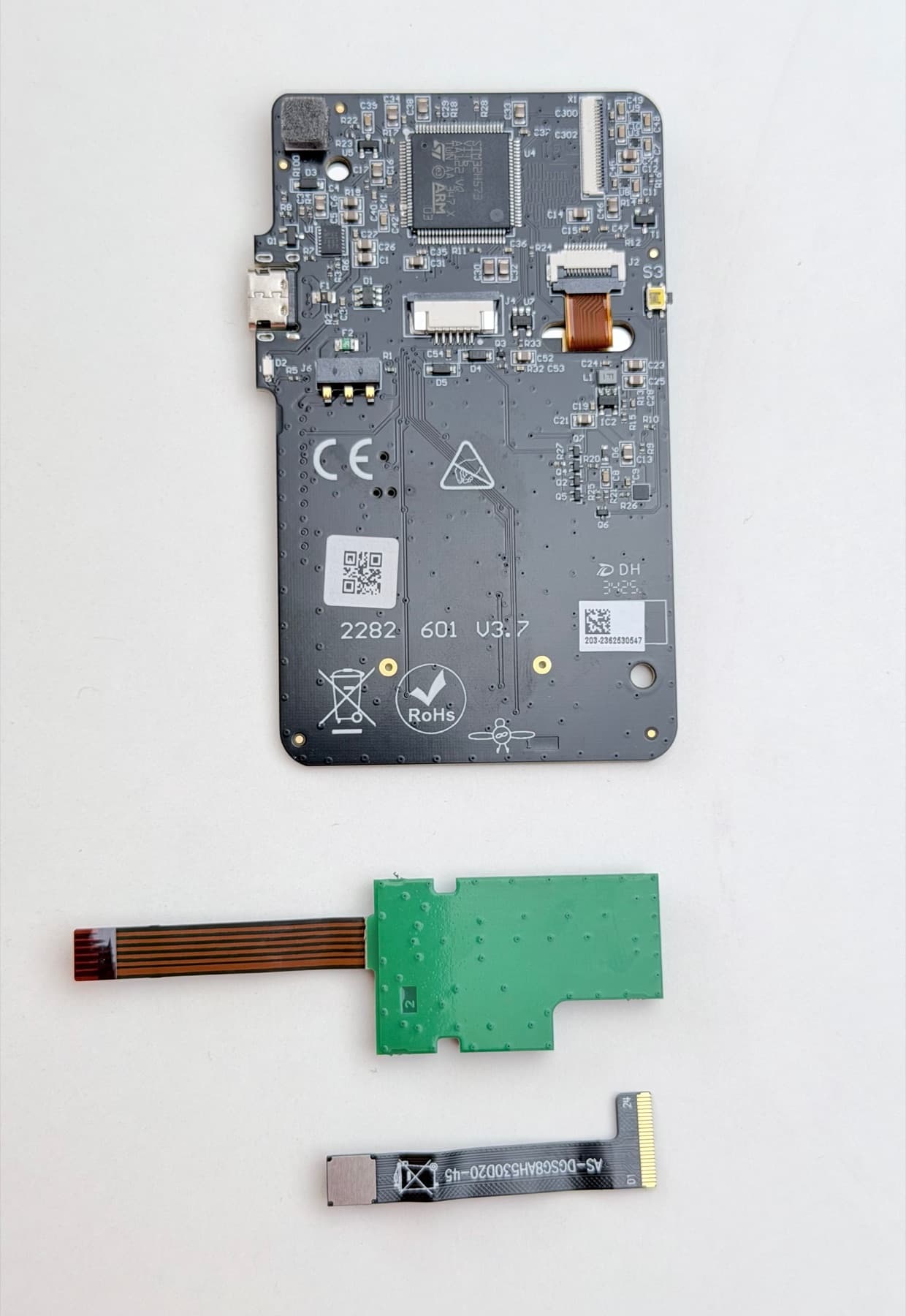
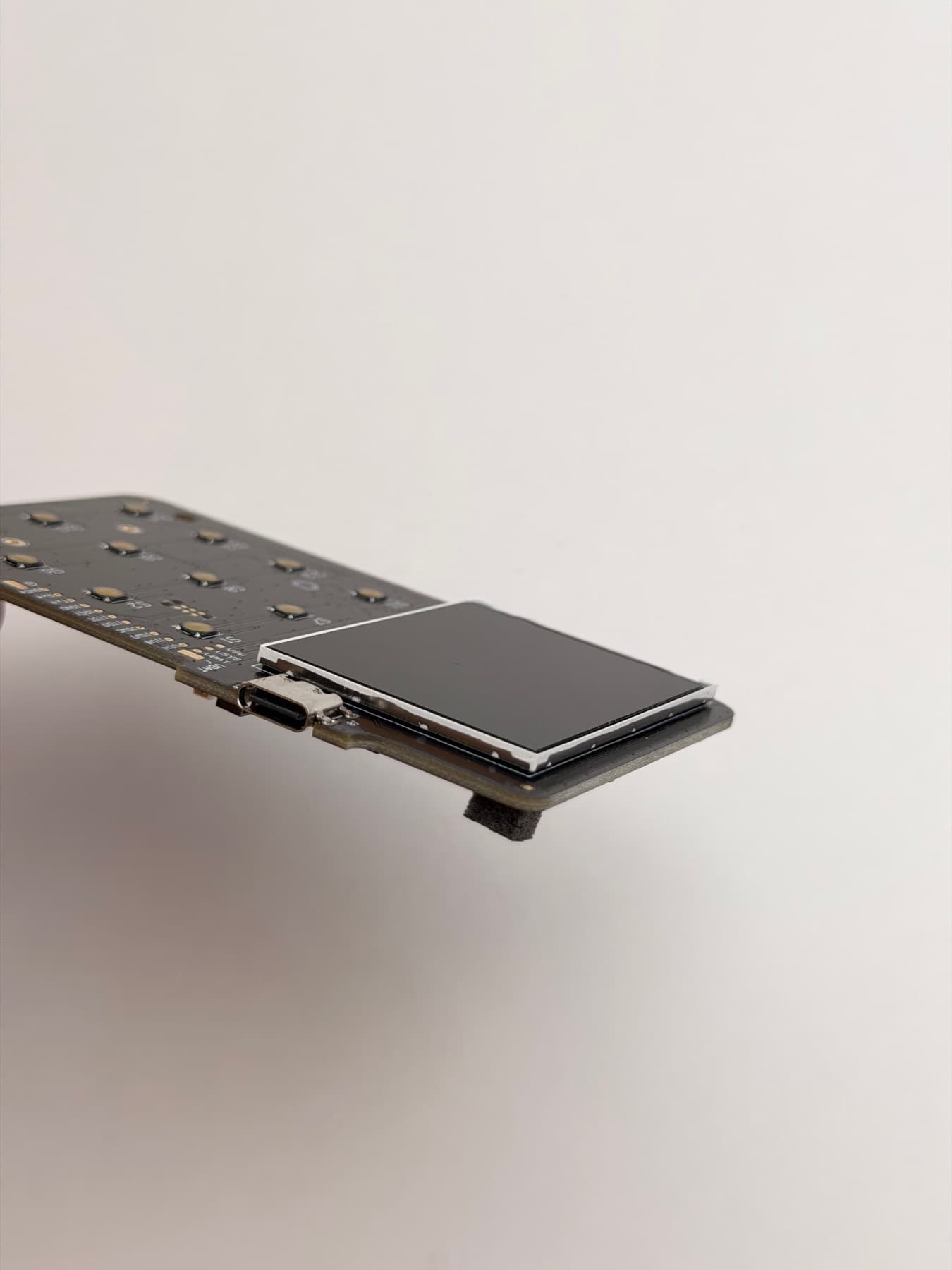
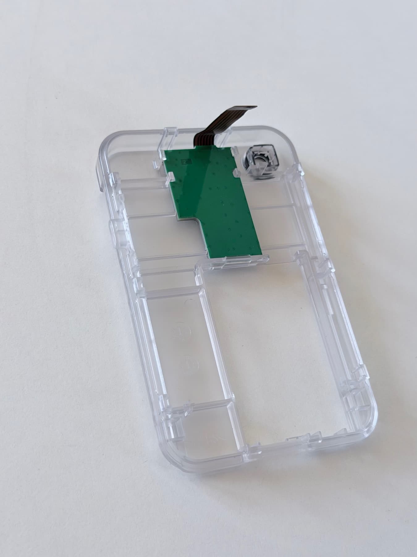
Compare your photos with the reference pictures below.
- A chip, component, or small board that is not in the reference pictures.
- Extra wires, or wires soldered onto the board.
- An antenna, a SIM or eSIM chip, or a wireless module. Shell has no radio: no Wi-Fi, no Bluetooth, no cellular. Any of these is a red flag.
- Fresh solder, flux residue, or glue where the reference pictures show none.
This picture shows all the components inside Keycard Shell.
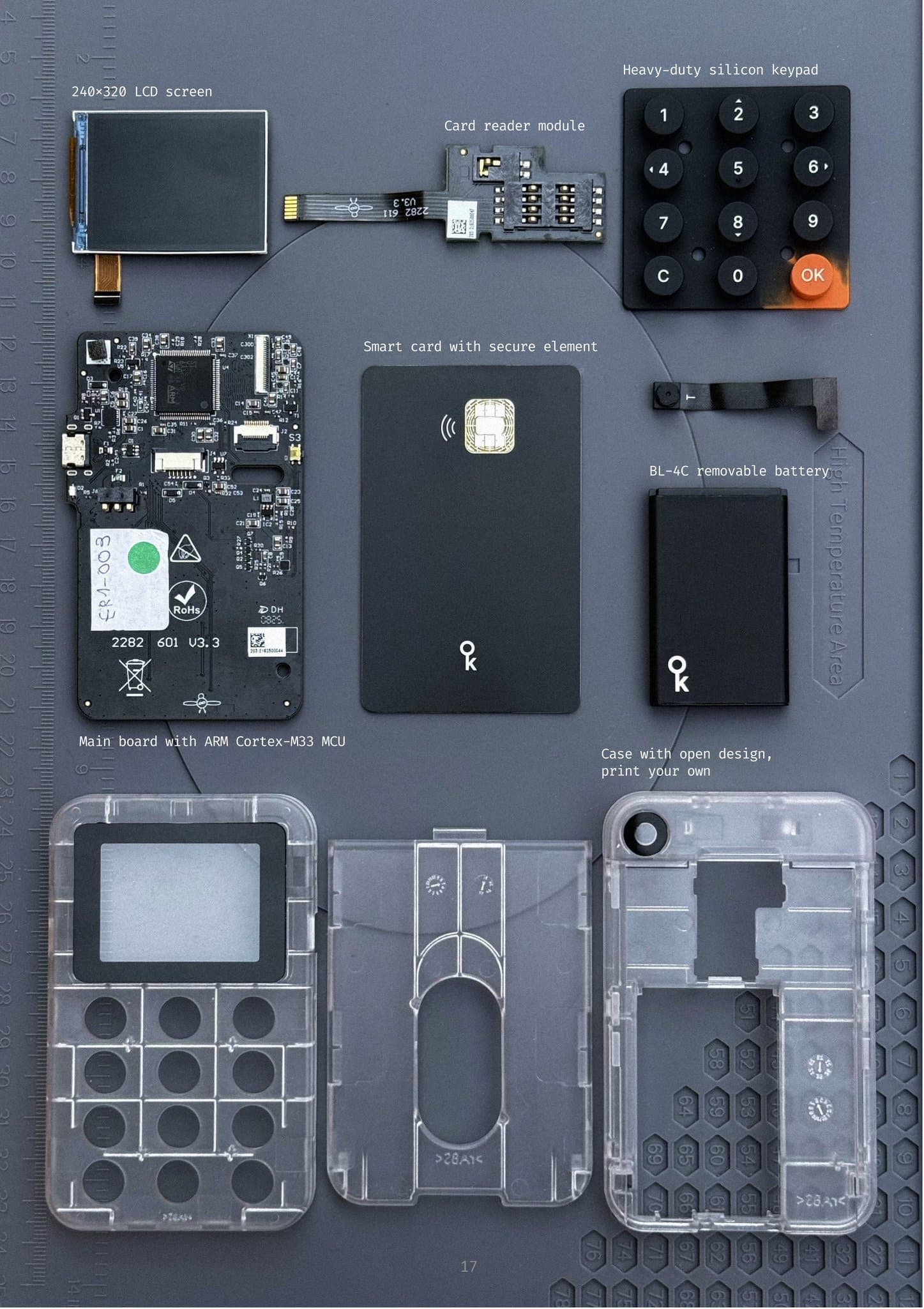
The PCB in this picture is version 3.3. It is not the production version (3.7). To compare your PCB, use the reference pictures below.
These pictures show a production Shell. Use them to check that your device has not been modified.
Watch the video to put your Shell back together.